 (China (Mainland))


Product Summary
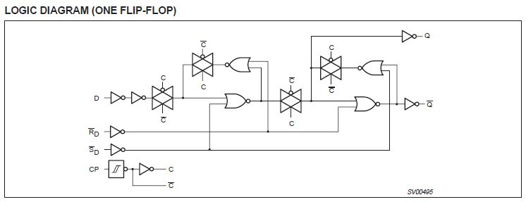
The 74LVC74APG is a high-performance, low-voltage Si-gate CMOS device and superior to most advanced CMOS compatible TTL families. The 74LVC74APG is a dual positive edge triggered, D-type flip-flop with individual data (D) inputs, clock (CP) inputs, set (SD ) and (RD ) inputs; also complementary Q and Q outputs.
Parametrics
74LVC74APG absolute maximum ratings: (1)DC supply voltage, VCC: 0.5 to +6.5V; (2)DC input diode current, VI<0, IIK: 50mA; (3)DC input voltage, VI: 0.5 to +5.5V; (4)DC output diode current, VO>VCC or VO<0, IOK: 50mA; (5)DC output voltage, VO: 0.5 to V+0.5V; (6)Storage temperature range, Tstg: 65 to +150℃; (7)Power dissipation per package, PTOT: 500 mW.
Features
74LVC74APG features:(1)Wide supply voltage range of 1.2V to 3.6V; (2)In accordance with JEDEC standard no. 8-1A; (3)Inputs accept voltages up to 5.5V; (4)CMOS low power consumption; (5)Direct interface with TTL levels; (6)Output drive capability 50 transmission lines @ 85℃.
Diagrams
 |
 74LV00 |
Other |
|
Data Sheet |
Negotiable |
|
||||||||||||
 |
74LV00BQ,115 |
NXP Semiconductors |
Gates (AND / NAND / OR / NOR) 3.3V QUAD 2-INPUT |
Data Sheet |
|
|
||||||||||||
|
74LV00D |
Other |
|
Data Sheet |
Negotiable |
|
||||||||||||
 |
74LV00D,112 |
NXP Semiconductors |
Gates (AND / NAND / OR / NOR) QUAD 2-INPUT NAND |
Data Sheet |
|
|
||||||||||||
|
74LV00D,118 |
NXP Semiconductors |
Gates (AND / NAND / OR / NOR) QUAD 2-INPUT NAND |
Data Sheet |
|
|
||||||||||||
|
74LV00DB,112 |
NXP Semiconductors |
Gates (AND / NAND / OR / NOR) QUAD 2-INPUT NAND |
Data Sheet |
|
|
||||||||||||
